
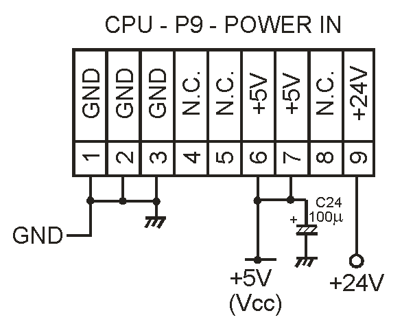
| |


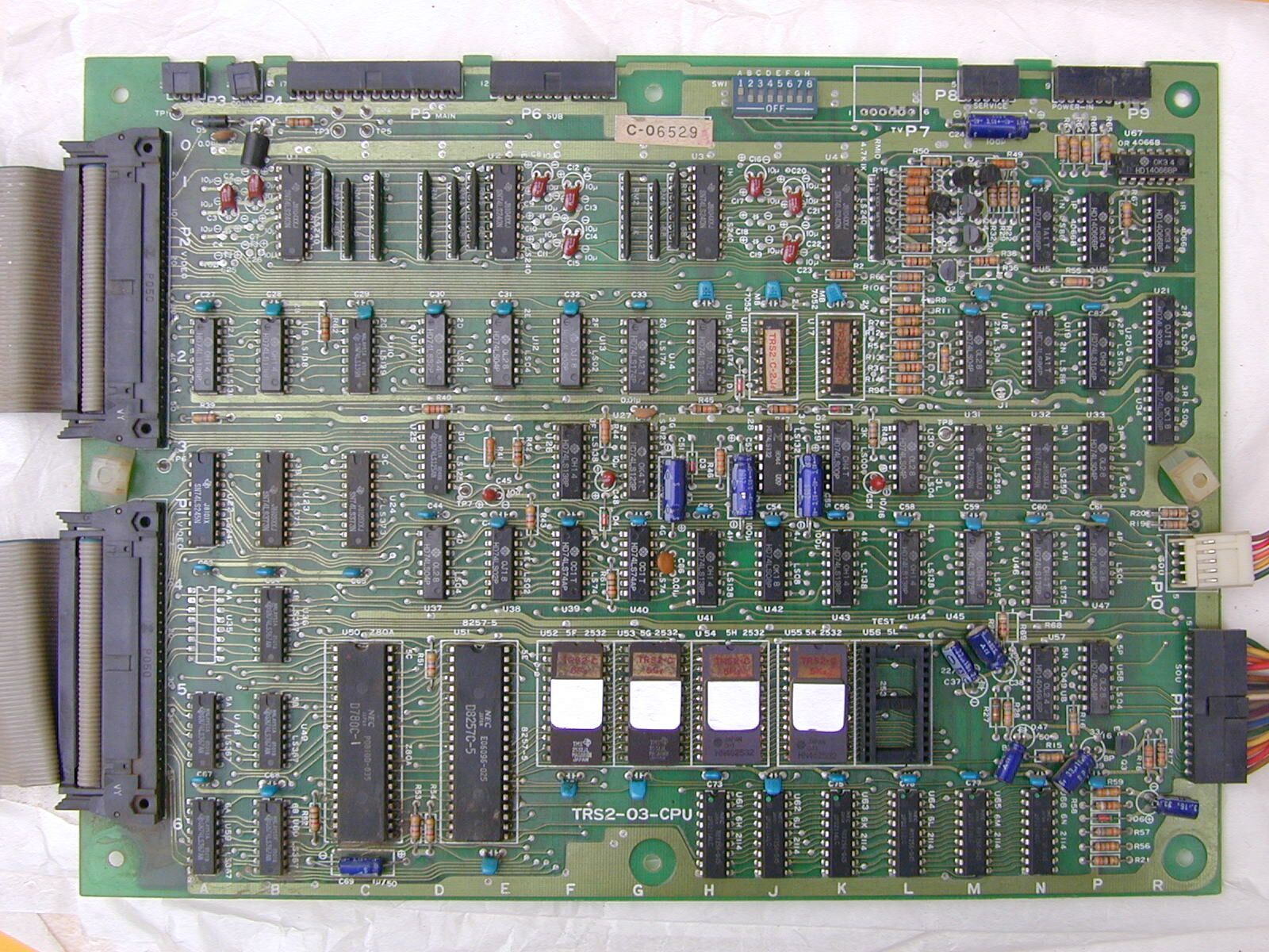
The Radar Scope CPU is a Z80 clocked at 3.072 MhZ. In the picture here
it is a NEC D780C-1, which is equivalent to a Z80-A (rated up to 4 MHz). On another
CPU board i see a Sharp Z80A soldered in. Additionally there is a DMA Controller
8257 on the board. The DMA controller is for the transfer of video data during
vertical blanks.
4 Program ROMS are of type 2532 (4K x 8 bit), which makes a total
of 16 K program code. For volatile storage there
is 3K RAM on the CPU board.
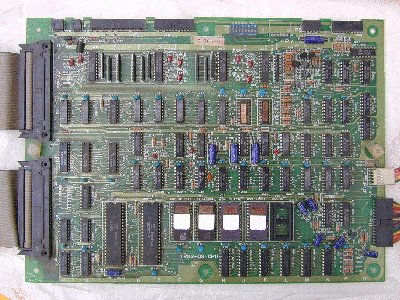 |
Click this picture to
enlarge CPU board. If you want to identify an unknown board and need a better picture, view this full sized CPU board image (size is 409 KB) |
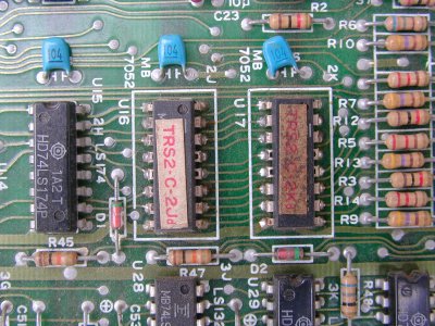
The color palette is created using these proms. This picture shows them on the CPU board.
How color generation works in theory is shown very nicely on the pages of Aaron Giles. He uses PacMan and Mappy as examples, but it works the same with Radar Scope.
These are 256x4 bit Proms used in parallel: An 8 bit address is applied
via the clocked flipflops 7474 at 2G and 2H. The 2J Prom then puts out
the red bits and the first green bit of the color information, the 2K
Prom the rest of two green and blue bits, respectively:
| Bit Position | 2J-D3 | 2J-D2 | 2J-D1 | 2J-D0 | 2K-D3 | 2K-D2 | 2K-D1 | 2K-D0 |
| Color | Red | Red | Red | Green | Green | Green | Blue | Blue |
If you need the color PROM contents for repairing your boardset with MB 7052 PROMS or a replacement (see below) they are referenced in this table:
| PROM location | Contents |
|---|---|
| 2J | trs2c2j.bin |
| 2K | trs2c2k.bin |
In one of my boardsets the color proms were missing. The color proms needed are MB 7052 PROMS, organized as 256 x 4 bit. Since i could not find a direct replacement for the MB 7052 PROMS i replaced them with GALs (Generic Array Logic). These are logic device IC's you can program (and reprogram) logic functions with. Basically you define what the inputs will be and what the outputs for each input state should be. I had no previous experience with this but it works great as a PROM replacement. Note: An EPROM can only be used if it is fast enough to handle the transfer speed. An old bipolar PROM is faster than an EPROM.
You need software and a programming device though. I used WinCupl
Version 5.2.16 (runs on Win95 and Win98, produces a JEDEC file) and an
ALL-03A Programmer to write the JEDEC file to the GAL (thanks George).
If you get an "Excessive number of product terms" error when compiling
you have to fiddle with the compiler options. I used the "Minimization:
Expresso" setting. You can also try to optimize the pin D3 separately
(with the TRS2-C-2K GAL).
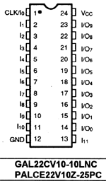 |
You might find some other similar GAL that works. Pin
CLK/I0 can be used as a clock input (not used here). The pins labeled
I1 to I11 are dedicated inputs. Pins I/O0 to I/O9 can be defined as
either inputs or outputs. For the replacement of a MB 7052 i used in
the case of the 2J PROM:
-Pins 2 to 9 are address inputs to the GAL -Pin 11 is used for the tri-state chip enable input -Pins 15 to 18 are outputs to the PROM socket Below is the wiring for the adapter you must build from the MB 7052 socket on the CPU board to the GAL. My programmer handles this GAL as manufacturer type "AMI" and device type "PEEL 22CV10". |
| This picture shows the necessary wiring for the 2J color PROM (as seen from top): | 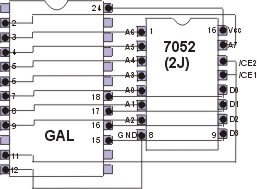 |
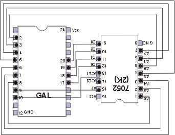 |
Also, there is a different layout for the pins: -Pins 2 to 9 are address inputs to the GAL -Pin 10 is used for the tri-state chip enable input -Pins 17 to 20 are outputs to the PROM socket |
| file | contents | comment |
|---|---|---|
| colprom.pld | logic source file for WinCupl | This is the pld file for the TRS2-C-2J color PROM. Compiler options: Expresso |
| colprom.jed | JEDEC file for programming the GAL | This is the file for the GAL programmer; TRS2-C-2J color PROM. |
| colpr_2k.pld | logic source file for WinCupl | This is the pld file for the TRS2-C-2K color PROM. Compiler options: Minimization: quick, MIN nibble = 4; in the file itself |
| colpr_2k.jed | JEDEC file for programming the GAL | This is the file for the GAL programmer; TRS2C-2K color PROM. |
The reset signal on power up is generated by the 74LS123 one shot at pos. 3G.
It can be observed at TP8.
If you need to reset the game often (as i do when troubleshooting), you probably
wish you had a reset button instead of powering off and on. Such a button is
not available, but you can easily create one.
I use a push button to clip onto the plus side of capacitor C53 (it is located
in the middle of the CPU board) and to ground (TP1), with a resistor, like this:
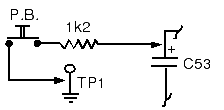
When you press the button for about 2 seconds, the game will reset.
The circuit below is easy to build and allows you to freeze the game in action. Then you can take screen pictures during attract mode or when a game is in progress and this can be very helpful for troubleshooting.
How it works: The Z80 CPU has six control signals for internal status and control of sequencing. Among them is the /WAIT (active LOW) signal input, normally used to synchronize (wait for) slow peripherals, like memory or I/O devices. In the picture below, this input is shown in the hatched area to the right:
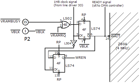
This is a section of redrawn schematics which shows the TRS01-CPU wait state control.
The video memory pulls the /WAIT input low to indicate that it is not ready for data transfer. The Z80 will then go into a wait state as long as /WAIT stays low.
At the time when /VRAMBUSY and /VRAMRQ both go low, the output of the NOR gate at 4E will go high. The 74LS74 flipflop is triggered by the positive edge of the CK input, so at the next clock pulse the input at D will cause Q be high and /Q be low, thus giving a low at the /WAIT input of the Z80.
During the vertical blanking interval (/VBLK is low) this flip flop will be forced to a state of Q = low and /Q = high, since the vertical blanking signal is connected to the /R (reset, active low) input of the flip-flop. This makes sense since the transfer to memory is done by DMA at this time (see explanation in 'the video system').
To hold /WAIT low and freeze the game we use a switch. Since mechanical switches do not allow for a clean transition from HIGH to LOW state this circuit debounces the switch:
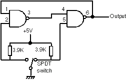 The
two NAND gates (here two gates from a 7400 for example) will lock each other
into a stable state once the SPDT switch has been thrown. This means that the
bouncing of the switch is prevented during those maybe two milliseconds when
the switch contacts do not close "cleanly".
The
two NAND gates (here two gates from a 7400 for example) will lock each other
into a stable state once the SPDT switch has been thrown. This means that the
bouncing of the switch is prevented during those maybe two milliseconds when
the switch contacts do not close "cleanly".
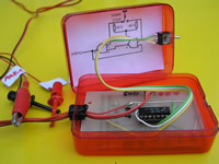 If
you put this device into a small plastic box with clips for +5 Volts supply
and GND and a cable for the output, you can connect its output to pin 6 of the
IC 74LS74 at position 4F. This goes directly to the WAIT input of the CPU. (You
could connect it directly at the CPU pin 24 but i found it easier to do at the
non-socketed flip-flop)
If
you put this device into a small plastic box with clips for +5 Volts supply
and GND and a cable for the output, you can connect its output to pin 6 of the
IC 74LS74 at position 4F. This goes directly to the WAIT input of the CPU. (You
could connect it directly at the CPU pin 24 but i found it easier to do at the
non-socketed flip-flop)
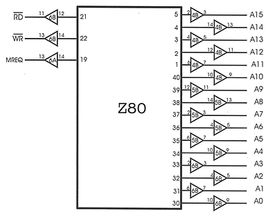
The address bus is buffered by 74LS367 Hex buffers as shown in this picture.
If you need to check the signals, the location of the buffer on the board is indicated, e.g. address line A10 is buffered in the buffer chip located at position 4B on the Radar Scope CPU board (pin 10 is the input, pin 9 is output).
The address bus is shown on the right and the memory control lines on the left. The numbers inside the rectangle are the Z80 pin numbers.
This is redrawn from the original schematics, since most numbers are hardly readable there.


