
| |


 |
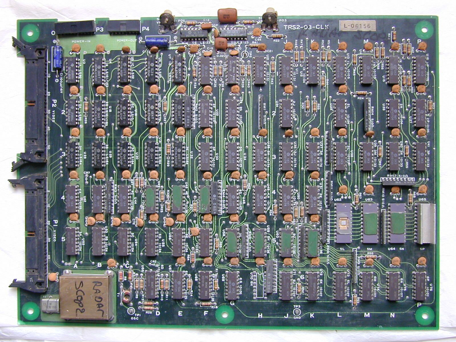
This is a Radar Scope CLK board (click on the picture to enlarge - 127 KB). Several of the heat fins on the ECL chips are missing and one of the ECL RAMS is even ripped open, exposing the die but - amazingly - this board is still working! If you need to identify an unknown board you can view this full
sized CLK board image (size is 410 KB) The CLK board provides basic timing functions:
|
|
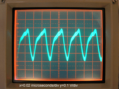
Signal on test point TP2, top middle of the board. Scope x=0.2 V/div; y=50µs.
|
The oscillator circuit is shielded under a small sheet brass box at the lower
left of the CLK board. The primary clock signal emerges at test point TP1 which
is connected to the small ferrite coil marked "T1".
Then it is connected to a 10116 ECL triple line receiver which is used to adapt
and buffer to the following two 10135 ECL dual J-K master slave flip-flops (position
6F). These two FF's divide the primary clock signal by 3, this signal (Ø3)
appears at 6F, pin 14 and is at (73.728 / 3 = 24.576 MHz).
|
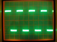
Ø3 clock signal at 6F, pin 14 (left side of ECL pull down resistor R18) |
The 1H signal (3.072 MHz) is going to the video board via connector P2-CLK, pin 46. There it is buffered and named 1HB. It leaves the video board on connector P4-CPU, pin 5 and goes to the cpu board where it is buffered again and finally becomes the clock for the Z80A on its pin 6.
|
| ||||||||||||||||||||||||
|
CLK power input
|
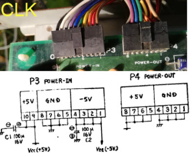 |
This is the upper left edge of a TRS2-03-CLK board, showing POWER IN (left) and OUT (on the right) connectors. See also in the power supply section. |


